Taiwan’s GlobalWafers is set to build a new semiconductor wafer factory in Texas, leveraging into the subsidies on offer from the new CHIPS Act signed into law by President Joe Biden on August 9.
GlobalWafers is expected to spend about US$2 billion on the facility initially and $5 billion eventually as wafer production, sales and profits rise. Demand should be supported by the construction of new factories by Intel, TSMC, Samsung and other semiconductor makers in the US.
According to a GlobalWafers statement on the investment, “At full build-out, the multi-staged, 3.2 million-square-foot silicon wafer factory will be the largest facility of its kind in the USA and among the largest in the world along with secured abundance of land to support any required further growth.”
It will also be the first such factory built in the US in two decades. The Taiwanese press reports that about 80% of the new factory’s initial capacity has already been booked in advance.
Headquartered in Taiwan, GlobalWafers ranks third among five companies that dominate production of silicon wafers for the semiconductor industry, with a market share of about 16% according to industry sources.
The other four are Shin-Etsu Chemical (30%) and SUMCO (24%) of Japan, Siltronic AG (13%) of Germany and SK Siltron (12%) of South Korea. The investment in new capacity follows the collapse of GlobalWafers’ attempt to buy Siltronic last February.


Chinese and smaller non-Chinese producers have only about 5% of the global market by value. The top five have factories in Japan, Taiwan, South Korea, Southeast Asia, Europe and America. In order to protect their intellectual property, none of the top five have built factories in China.
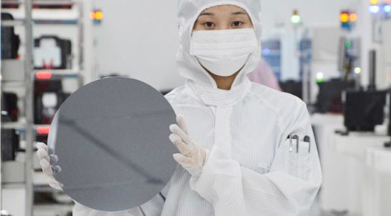
Silicon wafer fabrication depends on advanced technology. Like other parts of the semiconductor manufacturing process, wafer fabrication requires high-quality materials and precision equipment.
Silica (silicon dioxide, commonly found in nature as quartz) is first reduced to silicon metal in a furnace and refined into polycrystalline silicon of 99.99% purity.
In the most commonly used Czochralski process (invented by Polish scientist Jan Czochralski in 1915), the polycrystalline silicon is melted in a quartz crucible and doped with small amounts (a few parts per million) of boron, phosphorus or other dopants to create desired electrical properties.
A monocrystalline seed crystal is lowered into the molten silicon and then slowly raised at a steady rate while rotating. A cylindrical monocrystalline ingot grows around the seed crystal.
Ingots used to make 300-mm wafers can be up to two meters in length and weigh several hundred kilograms. An ingot puller can be nearly 9 meters tall and weigh 25 tons. The ingot is then segmented, ground to the required diameter and sliced into wafers less than 1-mm thick using a wire saw.
As explained by Siltronic, “A very thin metal wire, which can be many miles long, is pulled over the wire guide rollers in such a way that a wire web with very precise spacing is spanned. Nozzles apply the slurry to the web while the silicon ingot is slowly pushed through the web. This technology makes it possible to slice complete silicon ingots into hundreds of silicon wafers in just one step.”
The edges of the silicon wafers are then beveled (rounded) to prevent breakage and their surfaces lapped (ground with slurry) to make them parallel and remove any damage caused during slicing. The wafers are then cleaned, etched and polished.
Siltronic continues: “Based on polished wafers, epitaxial wafers feature an additionally deposited monocrystalline surface layer. They are essential for the manufacturing of highly integrated semiconductor Elements (ICs), image sensors (CIS), and certain power semiconductors.” The wafer is heated and the thin epitaxial layer (film) applied by means of vapor deposition.
Advanced logic devices manufactured by TSMC using 5-nm and smaller process technology and the CMOS image sensors made by Sony and others are built on epitaxial wafer substrates. Led by demand from TSMC and other foundries, epitaxial wafers are the fastest-growing segment of the semiconductor silicon market.


Keeping up with the technology and with market demand, which industry forecasters expect to grow at a mid-single compound annual growth rate for the next several years, is not cheap.
In addition to GlobalWafers’ large investment in the US, SUMCO has launched a $1.7 billion expansion in Japan and Taiwan. Shin-Etsu is also investing in those two markets to maintain its market share while SK Siltron plans to invest $1.1 billion to expand capacity in Korea. Siltronic is spending about $2 billion on a new ingot factory in Germany as well as a 300-mm wafer factory in Singapore.
It is in this competitive market environment that wafer makers in China are trying to get off the ground. Two Chinese wafer makers, TCL Zhonghuan Renewable Energy Technology and Zing Semiconductor, have recently featured in news reports about China’s efforts to catch up in chip production.
TCL Zhonghuan manufactures silicon materials for the solar power and semiconductor industries, including 200-mm and 300-mm polished and epitaxial silicon wafers. It also produces discrete semiconductor devices.
Zing’s efforts are focused on the production of silicon ingots and 300-mm polished and epitaxial wafers. According to its website, “It aims to build a production base, realize the localization for 300-mm silicon wafer, and fully meet the urgent demand of silicon substrates for large-scale integrated circuit production in China.”
Two small Japanese wafer makers also have production facilities in China. One of them, RS Technologies, formed a joint venture with China’s GRINM Group (the General Research Institute for Nonferrous Metals) in 2018. That venture is now producing silicon ingots and 200mm wafers. It plans to start production of 300mm wafers in 2023.
The other Japanese company, Ferrotec, has been making silicon ingots and 100mm, 150mm and 200mm wafers in China for many years. In 2021, having sold shares to Chinese investors to raise money for the project, it started making 300mm wafers. The build-out of 300mm wafer capacity will reportedly cost more than $1 billion.
All four companies contribute to China’s national semiconductor import substitution strategy and all four are eligible for Chinese government subsidies.


If all goes well, the country’s import substitution policy might enable them to raise China’s share of the global silicon wafer market to 10% by the end of the decade.
But unless Chinese electronic design automation companies and semiconductor equipment makers can get around US sanctions, they won’t have a chance at the leading edge.
If it accepts subsidies under the CHIPS Act, GlobalWafers will not be able to invest in China. Assessing market risk and opportunity, it has chosen to build its new factory in the US.
Follow this writer on Twitter: @ScottFo83517667