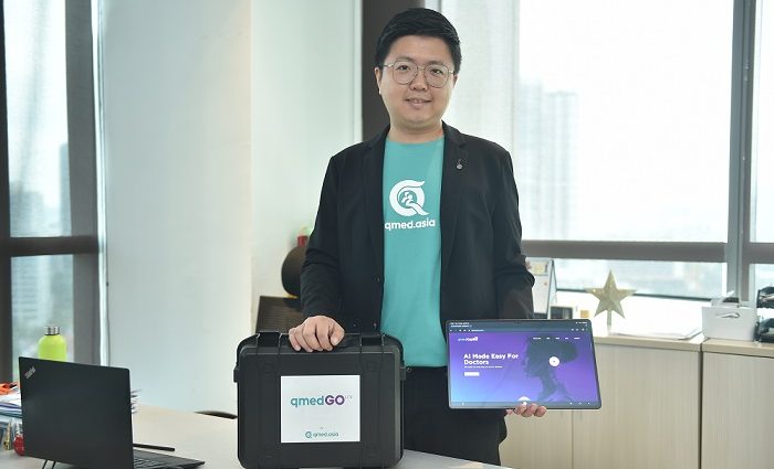
The long patient queues that triggered Dr Kev Lim’s startup journey to profitability with Qmed Asia

Family health challenge opened eyes to painful part of patient experience
Building a successful startup requires deep understanding of pain points

As a teenager growing up in Tangkak, Johor, Kev Lim took an interest in computing thanks to his older brother who was pursuing a degree in computer science. Helping himself to…Continue Reading

China fails Micron in security review

US-based Micron, the world’s third-largest maker of memory chips, failed a security review by the Cyberspace Administration of China, the government body announced May 21. “The review found that Micron’s products have serious network security risks, which pose significant security risks to China’s critical information infrastructure supply chain, affecting China’s national security,” an official statement said. No details were given.

Posters on Chinese news and social media sites viewed the measure as retaliation for American tech controls against China. “Those who want to eat Chinese food but want to smash the Chinese pot at the same time, should think clearly. This means that Micron will lose an important market,” wrote one commentator. “Companies that actively participate in the containment of the technology industry in mainland China, should think about it carefully.”

China announced the security review of Micron on March 31.

Continue Reading

APU SoMAD students and faculty win big at Wheel Rims Design Challenge

18 contestants secured spots in Top 32 for the competition
Three out of 18 contestants advanced to Top 10 positions

Beyond their crucial role in enhancing the overall driving experience, a rim design that harmoniously blends artistic elements with engineering becomes essential to satisfying one’s aesthetic desires.
Few know this better than Bryan Teh Yea…Continue Reading

Time to stop treating AIs like humans

The artificial intelligence (AI) pioneer Geoffrey Hinton recently resigned from Google, warning of the dangers of the technology “becoming more intelligent than us.” His fear is that AI will one day succeed in “manipulating people to do what it wants.”

There are reasons we should be concerned about AI. But we frequently treat or talk about AIs as if they are human. Stopping this, and realising what they actually are, could help us maintain a fruitful relationship with the technology.

In a recent essay, the US psychologist Gary Marcus advised us to stop treating AI models like people. By AI models, he means large language models (LLMs) like ChatGPT and Bard, which are now being used by millions of people on a daily basis.

He cites egregious examples of people “over-attributing” human-like cognitive capabilities to AI that have had a range of consequences.

The most amusing was the US senator who claimed that ChatGPT “taught itself chemistry.” The most harrowing was the report of a young Belgian man who was said to have taken his own life after prolonged conversations with an AI chatbot.

Marcus is correct to say we should stop treating AI like people – conscious moral agents with interests, hopes and desires. However, many will find this difficult to near-impossible. This is because LLMs are designed – by people – to interact with us as though they are human, and we’re designed – by biological evolution – to interact with them likewise.

Good mimics

The reason LLMs can mimic human conversation so convincingly stems from a profound insight by computing pioneer Alan Turing, who realized that it is not necessary for a computer to understand an algorithm in order to run it. This means that while ChatGPT can produce paragraphs filled with emotive language, it doesn’t understand any word in any sentence it generates.

The LLM designers successfully turned the problem of semantics – the arrangement of words to create meaning – into statistics, matching words based on their frequency of prior use. Turing’s insight echoes Darwin’s theory of evolution, which explains how species adapt to their surroundings, becoming ever-more complex, without needing to understand a thing about their environment or themselves.

AI still needs humans to survive and thrive. Image: Shutterstock / The Conversation

The cognitive scientist and philosopher Daniel Dennett coined the phrase “competence without comprehension”, which perfectly captures the insights of Darwin and Turing.
Another important contribution of Dennett’s is his “intentional stance.”

This essentially states that in order to fully explain the behavior of an object (human or non-human), we must treat it like a rational agent. This most often manifests in our tendency to anthropomorphize non-human species and other non-living entities.

But it is useful. For example, if we want to beat a computer at chess, the best strategy is to treat it as a rational agent that “wants” to beat us. We can explain that the reason why the computer castled, for instance, was because “it wanted to protect its king from our attack”, without any contradiction in terms.

We may speak of a tree in a forest as “wanting to grow” towards the light. But neither the tree, nor the chess computer represents those “wants” or reasons to themselves; only that the best way to explain their behavior is by treating them as though they did.

Intentions and agency

Our evolutionary history has furnished us with mechanisms that predispose us to find intentions and agency everywhere. In prehistory, these mechanisms helped our ancestors avoid predators and develop altruism towards their nearest kin.

These mechanisms are the same ones that cause us to see faces in clouds and anthropomorphize inanimate objects. No harm comes to us when we mistake a tree for a bear, but plenty does the other way around.

Evolutionary psychology shows us how we are always trying to interpret any object that might be human as a human. We unconsciously adopt the intentional stance and attribute all our cognitive capacities and emotions to this object.

With the potential disruption that LLMs can cause, we must realize they are simply probabilistic machines with no intentions, or concerns for humans. We must be extra-vigilant around our use of language when describing the human-like feats of LLMs and AI more generally. Here are two examples.

The first was a recent study that found ChatGPT is more empathetic and gave “higher quality” responses to questions from patients compared with those of doctors. Using emotive words like “empathy” for an AI predisposes us to grant it the capabilities of thinking, reflecting and of genuine concern for others – which it doesn’t have.

The second was when GPT-4 (the latest version of ChatGPT technology) was launched last month, capabilities of greater skills in creativity and reasoning were ascribed to it. However, we are simply seeing a scaling up of “competence”, but still no “comprehension” (in the sense of Dennett) and definitely no intentions – just pattern matching.

Artificial intelligence Photo: iStock
Actually, AIs aren’t very empathetic. Photo: iStock

Safe and secure

In his recent comments, Hinton raised a near-term threat of “bad actors” using AI for subversion. We could easily envisage an unscrupulous regime or multinational deploying an AI, trained on fake news and falsehoods, to flood public discourse with misinformation and deep fakes. Fraudsters could also use an AI to prey on vulnerable people in financial scams.

Last month, Gary Marcus and others, including Elon Musk, signed an open letter calling for an immediate pause on the further development of LLMs. Marcus has also called for an international agency to promote safe, secure and peaceful AI technologies” – dubbing it a “Cern for AI.”

Furthermore, many have suggested that anything generated by an AI should carry a watermark so that there can be no doubt about whether we are interacting with a human or a chatbot.

Regulation in AI trails innovation, as it so often does in other fields of life. There are more problems than solutions, and the gap is likely to widen before it narrows. But in the meantime, repeating Dennett’s phrase “competence without comprehension” might be the best antidote to our innate compulsion to treat AI like humans.

Neil Saunders is Senior Lecturer in Mathematics, University of Greenwich

This article is republished from The Conversation under a Creative Commons license. Read the original article.

Continue Reading

Malaysia Centre for 4IR to accelerate nation’s digital economy and green energy transition

Partners World Economic Forum to establish Malaysia Centre for 4IR
Thematic focus on digital transformation and green energy transition

The Centre for the Fourth Industrial Revolution Malaysia (Malaysia Centre for 4IR) was officially launched yesterday by the Minister of Economy, Rafizi Ramli and the President of the World Economic Forum (WEF), Børge Brende.
Hosted…Continue Reading

Samsung to jump-start Japan R&D, chip production

South Korea’s Samsung Electronics plans to establish a central research and development (R&D) facility and will likely build a semiconductor packaging test line in Japan, initiatives that come against the backdrop of a recent rapid improvement in bilateral ties and the ongoing US-driven “decoupling” of the global tech industry.

According to Japanese and Korean press reports, the world’s top producer of memory chips and second-ranking integrated circuit (IC) foundry plans to unify its R&D effort at its Yokohama Research Institute under the name Device Solution Research Japan (DSRJ). Samsung Electronics previously maintained half a dozen research facilities in Japan.

As reported by Pulse, DSRJ will hire Japanese as well as Korean researchers, an arrangement that should facilitate more interchange with Japanese suppliers and customers.

Pulse quoted an unidentified Korean business official as saying, “In the past, there was a perception that we have nothing more to learn from Japan, but Japan is still at the forefront of advanced technology. Samsung Electronics’ new integrated R&D center in Japan may signal the company’s intention to restore its link with Japan.” 

That is – or was – a popular sentiment in South Korea that had lots to do with historical resentment, but very little to do with commercial reality. Samsung and SK Hynix, South Korea’s other large semiconductor maker, have long depended on Japanese equipment and materials suppliers – and vice versa.

Over the past five years, Tokyo Electron – Japan’s largest and the world’s third-biggest supplier of semiconductor production equipment – has made nearly 20% of its sales in South Korea.

Japanese makers of photoresists and other chemicals used in the semiconductor manufacturing process – products in which they have dominant global market shares – also have substantial business in South Korea.

This became a political issue in 2019, when the South Korean Supreme Court ruled that Japanese companies must compensate Koreans forced to work for them during World War II.

Japan responded with export restrictions, causing massive inconvenience and disruption for both Korean customers and Japanese suppliers. Those restrictions were lifted in March of this year on the occasion of South Korean President Yoon Suk Yeol’s visit to Tokyo.

Prime Minister Fumio Kishida (R) shakes hands with South Korean President Yoon Suk Yeol (L) prior to the start of their meeting on March 16 at the Prime Minister’s Official Residence. Image: Twitter

According to DigiTimes, “Samsung stated that this organizational restructuring [of R&D in Japan] has nothing to do with the improvement of governmental relations between South Korea and Japan.”

In other words, it was reportedly a business decision grounded firmly in the company’s assessment of market conditions and opportunities.

In addition, Samsung is reportedly planning to build a test line for the development of new semiconductor packaging technology in Yokohama at a cost estimated at more than 30 billion yen (US$220 million).

This is an area in which Japanese equipment and material makers are particularly strong. Taiwan’s TSMC, the world’s leading IC foundry, opened a 3D IC packaging R&D center in Japan’s Tsukuba Science City almost a year ago. More than 20 Japanese materials and equipment companies are working with TSMC in Tsukuba.

Construction of the packaging facility should start this year, according to press reports, with operation scheduled to begin in 2025. Several hundred people are likely to be employed. Like TSMC and US memory chip maker Micron before it, Samsung is expected to receive generous government subsidies to build semiconductor production facilities in Japan.

Samsung did not provide comments for the story but the amount of detail and the fact that it was front-page news in Japan suggests that there is something to it.

Last December, Samsung established an AVP (Advanced Package) Business Team within its Device Solutions Division. Working with its Japanese suppliers at a prototype development facility in Yokohama would be a logical next step.

If TSMC needs to be in Japan to get the most out of Japanese packaging technology, Samsung probably does as well. Samsung’s foundry business is still only one-third the size of TSMC’s.

This would be Samsung’s first semiconductor production facility in Japan and a major step forward in the collaboration between the two countries’ semiconductor industries. Sony is a customer of Samsung Foundry but production is done in Korea. TSMC, Sony and Toyota Group components maker Denso are building a semiconductor factory in Kyushu, Japan.

Advanced packaging aims to overcome the physical limits of miniaturization – to go beyond Moore’s Law, the prediction made in 1965 by Intel co-founder Gordon Moore that the density of transistors on an integrated circuit would continue to double roughly every two years.

In Samsung’s words:

“Through advanced Heterogeneous Integration, which connects multiple chips horizontally and vertically, more transistors can be planted on a single chip (or package) and offer performance that is more powerful than the sum of all parts.”

“Our focus areas are the development of next-generation 2.5D and 3D advanced package solutions based on RDL, Si Interposer/Bridge and TSV stacking technologies.”

These technical terms are defined as follows:

  • 2.5D package: A package which integrates a single-layer logic semiconductor and multi-layer memory semiconductor together on a substrate.
  • 3D package: a package in which multiple logic/memory semiconductors are vertically integrated.
  • RDL (Redistribution Layer): Advanced packaging technology that places an extra metal layer in between a small and large circuit board to integrate the two.
  • Si Interposer/Bridge: The microcircuit board inserted between the IC chip and PCB, which physically connects the chip and board by acting as the mid-level wiring.
  • TSV (Through Silicon Via): Advanced package technology that grinds the surface of the chip, drills hundreds of microscopic holes and connects the electrodes that vertically penetrate the holes in the top and bottom chips.

Samsung’s advanced packaging also includes chiplets, which are “small, modular chips that can be combined to form a larger, more complex system-on-a-chip (SoC).

They offer a number of benefits over traditional monolithic chips, including improved performance, cost savings, and design flexibility,” according to industry information service anysilicon.

Along with die shrinks to 3nm and below, advanced packaging is the leading edge of semiconductor production technology.

South Korean President Yoon and Japanese Prime Minister Fumio Kishida are scheduled to meet during the G7 Summit in Hiroshima, scheduled to be held May 19-21. More information about Samsung’s investments and other economic collaboration between South Korea and Japan may be announced at the event.

Follow this writer on Twitter: @ScottFo83517667

Continue Reading

GBS Asia Awards 2023 Honors Organisations and individuals in the GBS industry

12th installment of awards sees 70% increase in nominations
6 new categories with judging by independent panel from M’sia & abroad

Global Business Services (GBS) Malaysia, a chapter of PIKOM, recently held its annual award ceremony to celebrate companies and individuals that found success using the GBS models. 
“Despite the effect of COVID-19 on the…Continue Reading

Malaysia faces escalating cybersecurity breaches and skills gap: Fortinet Survey

45% of respondents experienced breaches costing over US$1mil in past year
No single org or entity can solve problem alone, vital role for govts to play 

Image source: 2023 Fortinet-IDC Asia Pacific SASE Survey
A recent Asia-Pacific SASE survey commissioned by Fortinet from IDC revealed that 45% of Malaysian respondents experienced breaches costing over US$1 million in…Continue Reading