Malaysia’s tech education space sees entry of Rocket Academy from Singapore

Platform caters to recent graduates to seasoned working adults
Help career switchers, tech enthusiasts learn coding for software engineering jobs

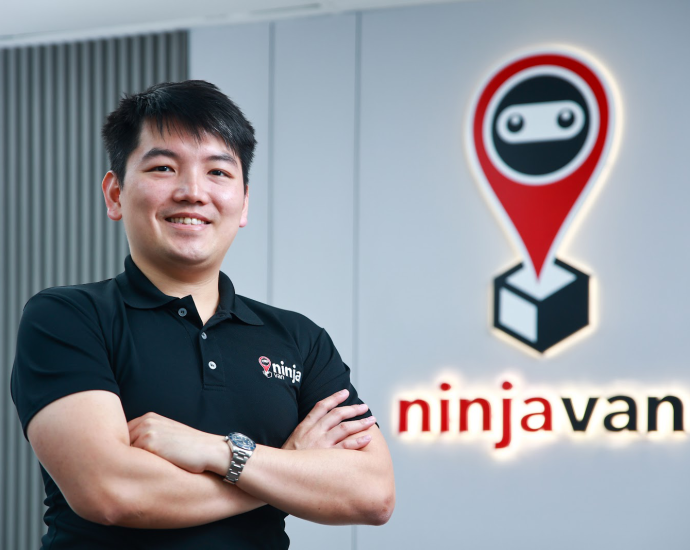
Malaysia’s journey of digital transformation is progressing, with the digital economy predicted to contribute 25.5% of Malaysia’s GDP by 2025. Additionally, with job vacancies registering a year-on-year increase of 29.3%, this is an…Continue Reading

Samsung to build all-AI, no-human chip factories

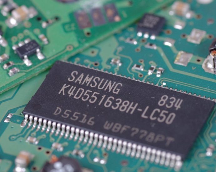
Samsung Electronics is planning to fully automate its semiconductor factories by 2030, with “smart sensors” set to control the manufacturing process, according to South Korean media reports.

The world’s largest maker of memory chips aims to create an “artificial intelligence fab” that operates without human labor, the reports said. The ground-breaking project is reportedly already underway, the same reports said.

Samsung has signaled since last summer it aims to AI to optimize integrated circuit (IC) design, materials development, production, yield improvement and packaging. Identifying the cause of defects in the production process is reportedly a top priority of the AI plan.

Samsung is developing its own sensors and switching procurement from foreign to domestic suppliers to gain control of the technology and develop relevant South Korean expertise. Measuring plasma uniformity in deposition, etching and cleaning is one key application; real-time monitoring of production processes is another.

The technology will be applied both to Samsung’s DRAM and NAND flash memory operations and its contract manufacturing operations. Catching up with Taiwan’s TSMC and staying ahead of America’s Intel are of vital importance to Samsung as die-shrinks progress from 3nm now to 2nm by 2025 and 1nm late in the decade.

The finer the circuit line widths, the greater the risk of microscopic defects dragging down chip production yields. Deploying AI to keep the problem to a minimum is increasingly critical to maintaining competitiveness. A completely automated factory would also eliminate the risk and cost of human contamination.

Top-end chips are expected to come down to 1nm by the end of the decade. Image: Facebook Screengrab

Samsung’s new sensors are reportedly small enough to fit on existing production lines, enabling the upgrade of current facilities while saving space.

This is important because Samsung currently has the largest wafer processing capacity in the semiconductor industry with more than a dozen production lines in South Korea, China and the US. All of the facilities are reportedly candidates for smart sensor upgrades.  

Samsung is preparing to build a new chip factory in Texas and plans to add five new “state-of-the-art” production lines in South Korea by 2042 at a total cost of about 300 trillion won (US$230 billion).

The five domestic lines will be built at a new industrial complex in Yongin, south of Seoul, where Samsung will work with about 150 suppliers, IC design companies and research institutions. Those facilities are likely to be completely automated.

Last March, the South Korean government issued a statement saying, “The mega cluster [in Yongin] will be the key base of our semiconductor ecosystem… [to] leap forward as a leading country in the middle of fierce global competition over advanced industries.”

“Timing is everything in the semiconductor industry,” Samsung Semiconductor CEO Kyung Kye Hyun said according to reports. “It is most important to start the construction of the Yongin National Industrial Complex early to maintain dominance amid intensifying global semiconductor competition.”

Samsung is also building a new semiconductor R&D center in Yongin. When he visited the site last October, Samsung Electronics Executive Chairman Lee Jae Yong said, “We need a turning point for innovation that leads us to take another leap in the semiconductor business amid ongoing internal and external risks.”

Samsung Electronics expects to report operating profits for the fourth quarter of 2023 of between 2.7-2.9 trillion won, which would be an increase of 11% to 19% over third-quarter profits. Sales are expected to remain more or less unchanged, but memory prices have started to recover while costs come down.

Despite global macroeconomic uncertainty, Samsung’s management expects continued improvement in chip market conditions in 2024. Higher sales and profits, in turn, will make it easier to fund the automation of existing production lines and the construction of new AI-powered factories.

Samsung kept semiconductor capital spending roughly flat in 2023 amid a cyclical downturn. In 2024, the company should resume its long-term upward investment trend, with a focus on increasing the production of high-bandwidth memory used with AI accelerators.

South Korea’s SK Hynix is also deploying more AI in its chip-making mix. Photo: Asia Times Files / AFP / Jung Yeon-Je

AI is both a productivity-enhancing tool and a new growth market for memory chip makers like Samsung, SK Hynix and Micron. SK Hynix is working with Gauss Labs, an industrial AI solutions developer with offices in Palo Alto, California, and in Seoul.

The AI start-up’s “Panoptes virtual metrology” solution is already being used to optimize thin film deposition in SK Hynix factories and more applications are reportedly in the pipeline.

Micron, meanwhile, has its own internally developed AI to optimize production. “We have built something here that is completely differentiated. We’re seeing much, much higher levels of accuracy,” said Koen de Backer, Micron’s vice president of smart manufacturing and AI.

“We can now launch products twice as fast while improving productivity by 10%. It’s truly been transformative. You could say it’s a killer app,” the Micron executive claimed.

With that competition, Samsung’s completely automated AI fab is a strategic imperative, not an option, in a chip-making landscape fastly being reshaped by AI.

Follow this writer on X: @ScottFo83517667

Continue Reading

CelcomDigi partners Japan’s SoftBank Corp and SC-NEX for AI-enabled and robotics solutions

Allows Malaysian enterprises to unlock the true potential of their businesses
Rely on CelcomDigi to improve productivity, strengthen business resilience

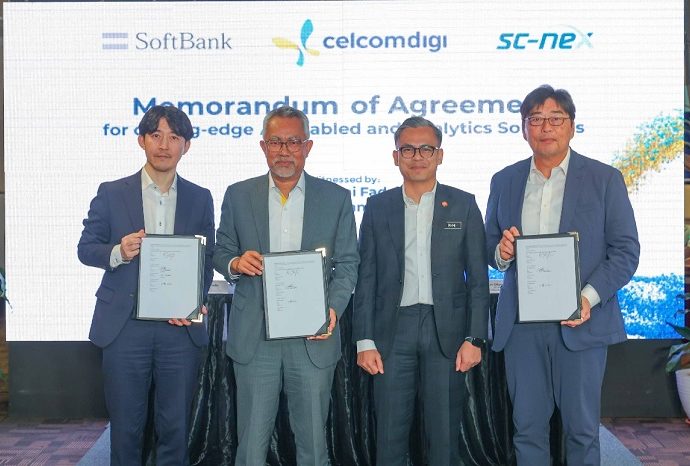
CelcomDigi Bhd announced a strategic partnership with two global technology organisations – SoftBank Corp, a telecommunications and IT corporation headquartered in Tokyo, and SC-NEX, a Sumitomo Corporation company – to accelerate the digitalisation…Continue Reading

Capgemini: Majority of business leaders optimistic about their growth in 2024

83% plan to increase investments in digital tools and technology, in particular AI
50% see climate change as biggest driver of operational disruption over next decade

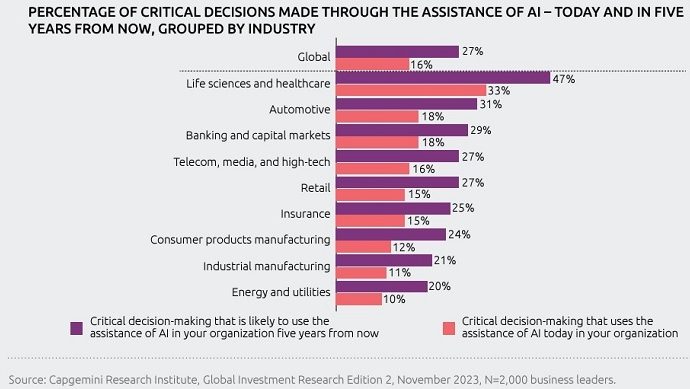
Business leaders are starting 2024 with an increased level of optimism about their organization’s future growth compared to 12 months ago, according to a report released today….Continue Reading

Rohm, Quanmatic putting quantum tech in chipmaking

Japanese chip maker Rohm is collaborating with venture company Quanmatic to improve electrical die sorting (EDS) in what appears to be the first use of quantum computing to optimize a commercial-scale manufacturing process on semiconductor production lines.

After a year of effort, the two companies have announced that full-scale implementation of the probe test technology can begin in April in Rohm’s factories in Japan and overseas. Testing and validation of the prototype indicate that EDS performance can be improved by several percentage points, improving significantly productivity and profitability.

Headquartered in Kyoto, Rohm produces integrated circuits (ICs), discrete semiconductors and other electronic components. It is one of the world’s leading suppliers of silicon carbide wafers and power management devices used in electric vehicles (EVs) and various industrial applications.

Quanmatic is a Japanese venture company that develops software incorporating algorithms for quantum computing efficiency and precision. Its computational optimization engines leverage quantum technologies for business and industry problem-solving.

EDS is conducted after wafer processing to identify defective chips, which are repaired or removed before cutting the wafer into individual chips and packaging. The process is key to improving and maintaining yields.

EDS is done by putting the wafer in contact with a probe card, an electrical-mechanical interface that can have more than 50,000 tiny needles that send electrical signals through the wafer to determine if the chips work properly and sort out those that do not. Doing this after chips have been packaged would be inefficient and expensive.

With the advance of semiconductor fabrication technology, EDS has become extremely complex, making it increasingly difficult to find a solution that optimizes the manufacturing process.

To address the problem, Rohm and Quanmatic developed an operating system that combines quantum and classical computation with Rohm’s semiconductor manufacturing data and decades of experience.

The two companies note that quantum technology – in particular quantum annealing – has recently been introduced in various fields for combinatorial optimization, with delivery route optimization as one prominent example.

Progress in chip manufacturing technology has seen an exponential increase in the number of possible EDS combinations. Meanwhile, various physical and process constraints make it difficult to find an optimal EDS solution.

In the words of BlueQubit, a quantum software developer based in Los Angeles, “…quantum annealing is an advanced computational method that uses quantum mechanics to solve optimization problems more efficiently than classical computers.

It’s like a superpowered search engine designed to scour an enormous solution space and pinpoint the optimal solution with a level of speed and accuracy that other computing models simply can’t match.

Its ability to handle problems of scale and complexity beyond traditional computing capabilities… paves the way for unprecedented innovations in various industries.”

The term was introduced by Diego de Falco, Nicolo Cesa-Bianchi and B Apolloni of the University of Milan in 1988, but Hidetoshi Nishimori of the Tokyo Institute of Technology and his student Tadashi Kadowaki are given credit for the model of quantum annealing that sparked the quantum computing boom ten years later.

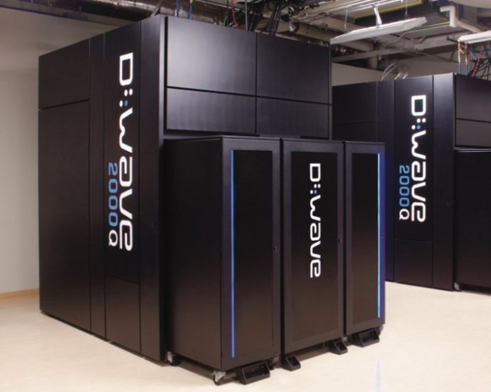
Quantum annealing was first commercialized by the Canadian company D-Wave Systems in 2011. Headquartered in Burnaby, British Columbia, D-Wave provides quantum computing systems, cloud services and software for use in manufacturing, logistics, financial services, life sciences and other industries.

A D-Wave quantum annealer. Image: X Screengrab

Its customers include Volkswagen, supermarket operator Pattison Food Group, advertising company Interpublic Group, BBVA, Lockheed Martin and, in Japan, Toyota, Denso and NEC. D-Wave has an office in Tokyo.

Professor Nozumu Togawa of Waseda University was also inspired by the work of Nishimori and Kadowaki, and D-Wave’s example.

He and three others – Keio University Associate Professor Shu Tanaka, former Dell Technologies and McKinsey & Company strategist Sumitaka Koga and Waseda engineering graduate Yosuke Mukasa – founded Quanmatic in 2022.

Togawa is chief scientific officer, Tanaka is chief technology officer, Koga is CEO and Mukasa is in charge of products. Togawa calls Quanmatic’s work with Rohm “an example of a highly mathematical optimization calculation method researched at a university being applied in the real world.”

Tetsuo Tateishi, board member and chief technology officer at Rohm says:

As the role of semiconductors becomes increasingly important to achieving a decarbonized society, ensuring stable supply has become a societal issue. The development of an operational system suitable for large-scale mass production lines using quantum technology represents a major step forward for the semiconductor manufacturing industry, enabling real-time optimization of production processes.

Going beyond the current situation, we will accelerate the introduction of quantum technology and related methods into a wide range of processes, with the goal of strengthening our stable supply system by establishing a more holistically optimized supply chain.

That’s an admirable aspiration, but if its application to EDS lives up to expectations, quantum annealing will first make an important contribution to Rohm’s competitiveness and eventually be adopted throughout the semiconductor industry.

Follow this writer on X: @ScottFo83517667

Continue Reading

MEASAT to distribute Starlink services to its 130 markets

Authorised reseller status enables MEASAT to expand product options
SpaceX to tap a well established 24×7 technical on-ground network

MEASAT Global Bhd – a Malaysian satellite solutions provider has officially signed with Space Exploration Technologies Corp (SpaceX) to become the official authorised reseller for Starlink Hardware and Services in the markets that…Continue Reading

Uni students win big at Hong Leong Bank’s generative AI hackathon

‘Can You Hack It’ saw solutions to improve customer & workplace experience
Alignment with HLB brand values which strongly promote a culture of innovation

Hong Leong Bank (HLB) organized Malaysia’s first Generative AI-themed hackathon in Dec, with its sixth annual ‘HLB Can You Hack It’ hackathon. With 90 teams of students, fresh graduates,…Continue Reading

Penang’s startup ecosystem receives recognition with Georgetown as 8th ranked city in Southeast Asia 

Georgetown is 2nd highest-ranked city in Malaysia with KL at 4th spot
Supporting startup ecosystem part of plan to attract high-tech industries

In a statement, Digital Penang marked a significant milestone for Penang’s technology startup ecosystem as it received the “Outstanding Ecosystem among Medium-Sized Population Cities in Southeast Asia 2023” award from StartupBlink, a leading startup…Continue Reading