Foxconn, Nvidia joining hands to forge AI industrial revolution

Taiwan’s Hon Hai Technology Group, widely known as Foxconn, and America’s Nvidia plan to join technological forces “to accelerate the AI industrial revolution.”

Foxconn, the world’s largest contract manufacturer, is the primary assembler of the Apple iPhone. California-based Nvidia is the world’s leading designer of the graphics processing units (GPUs) used in artificial intelligence applications.

Foxconn intends to use Nvidia technology to further the digitalization of manufacturing and inspection workflows, the development of AI-enhanced electric vehicles and robotics, and language-based generative AI services.

Both tech giants are in pursuit of new growth opportunities as Foxconn diversifies away from its traditional heavy dependence on Apple and Nvidia seeks new markets amid US government sanctions that have crippled its once-booming business in China.

However, Nvidia said this month it has developed three new sanctions-compliant AI chips, based on its flagship H100 product, for China’s markets.

Foxconn chairman and CEO Young Liu and Nvidia CEO Jensen Huang revealed their collaborative revolutionary plans on October 18 at the Hon Hai Tech Day event held in Taipei.

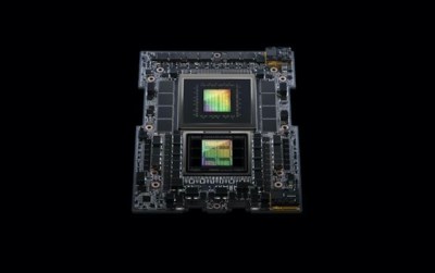
They reportedly plan to build factories supported by Nvidia GPU-based computing infrastructure designed to process, refine and transform large amounts of data into AI models that can identify patterns and make predictions. These new data centers will be based on Nvidia GH200 Grace Hopper Superchips and AI enterprise software.

The GH200 Grace Hopper system-on-chip (SoC) combines Nvidia’s Grace central processing unit (CPU) and Hopper GPU architectures with high-bandwidth memory to enable large-scale AI training, inference and high-performance computing.

Launched in August 2023, the GH200 was created to handle the most complex generative AI workloads including large language models, recommender systems (AI algorithms associated with machine learning) and vector databases (data stored as mathematical representations to facilitate machine learning).

Nvidia has unveiled a new variant of its GH200 superchip,’ which is set to be the world’s first GPU chip to be equipped with HBM3e memory. Image: Nvidia

Huang noted that “A new type of manufacturing has emerged… Foxconn, the world’s largest manufacturer, has the expertise and scale to build AI factories globally.”

Foxconn will also use Nvidia technology in other industrial and infrastructure solutions, the arguably most impressive of which is Foxconn’s Smart EV. Built on the Nvidia Drive Hyperion 9 platform for autonomous vehicles, it will be powered by Thor SoC computer, which enables automated and assisted driving, parking, driver and passenger monitoring, digital instruments and in-vehicle information and entertainment systems.

Scheduled to be introduced in 2027, Hyperion 9 will support level 3 conditional urban passenger car driving, characterized as hands-off, eyes-off but ready to resume control, and level 4 advanced highway driving, characterized as “brain-off”, no need to pay attention.

Foxconn has been working on EVs for several years. It has only a small presence in the industry today but has ambitious designs. By 2027, it aims for 10% of the global market for EV components and services. It has a test satellite in low Earth orbit and plans to integrate satellite communications with the Internet of Vehicles (IoV) in the not-too-distant future.

Foxconn Smart Manufacturing robotic systems will be built on the Nvidia Isaac autonomous mobile robot platform, which runs the gamut from training, simulation and building of autonomous robots to robot fleet management.

Foxconn Smart City will incorporate Nvidia Metropolis video analytics, which are designed to “make sense of the flood of data created by trillions of sensors” in traffic management, retail logistics, healthcare and other urban services. 

The timing is seemingly right. Nvidia points out that “Advances in edge AI and simulation are enabling deployment of autonomous mobile robots that can travel several miles a day and industrial robots for assembling components, applying coatings, packaging and performing quality inspections.”

These robots are arriving just as demographic change creates a chronic shortage of workers in China and other advanced industrial nations.

Foxconn is already the largest manufacturer of Nvidia-based AI hardware, according to market research and electronics industry media sources. In addition to selling hardware to and building systems based on Nvidia technology for its customers, Foxconn plans to use the technology in its own factories to improve efficiency while saving time and money.

Outside Taiwan, Foxconn has manufacturing, design and R&D facilities in more than 20 countries and regions including China, India, Japan, Vietnam, Malaysia, Australia, Czech Republic, Slovakia, Hungary, the US, Mexico and Brazil. This, along with more than 40% of the global market for electronics manufacturing services, gives it a reach that its competitors will find difficult to match.

Foxconn Industrial Internet, a group subsidiary headquartered in Shenzhen, China, serves markets for smartphones and smart wearable devices, smart homes, cloud and edge computing, 5G and other network communication devices, EV and other new energy vehicle components, and the industrial internet. Established in 2015, Foxconn Industrial Internet has about 200,000 employees, almost as many as China tech giant Huawei.

Unlike Huawei, which is under US tech war-related sanctions, Foxconn is welcome in all of the world’s major markets. It has a factory in the US state of Wisconsin and runs one of the largest foreign-owned factories producing for export, known as maquiladoras, in Mexico.

The Foxconn facility was at one point expected to bring in $10 billion of investment and create 13,000 jobs in Wisconsin. Photo: Handout

In August 2023, Foxconn and the Chihuahua state government in Mexico announced a partnership aimed at increasing the state’s industrial capabilities by training workers for the information & communications and auto industries, optimizing supply chains, improving infrastructure, raising energy efficiency and furthering the development of renewable energy.

Foxconn has so far invested more than US$500 million in Chihuahua, which borders the US states of New Mexico and Texas. It has production facilities there, in Ciudad Juarez and also in Tijuana, south of San Diego.

Foxconn’s factory in Wisconsin, promoted heavily by former president Donald Trump, has been scaled back and is generally regarded as having been a politically motivated investment aimed at evading tariffs. Under the US-Mexico-Canada Agreement, formerly known as NAFTA, that can be done much more economically from Mexico.

Follow this writer on Twitter: @ScottFo83517667

Continue Reading

MRANTI opens Malaysia’s largest AV experimental lab

Next-generation freedom and automatic vehicle innovation3 staged evaluations, data security, and securityThe largest multi-scenario autonomous vehicle ( AV ) experimental laboratory in the nation, AV XL, was introduced today by MRANTI through the Ministry of Science, Technology, and Innovation ( MOSTI).In order to hasten the growth of Malaysia’s mobility industry, MRANTI…Continue Reading

EdgePoint Infrastructure reaches 1,500 towers milestone in Malaysia 

Edgepoint is ranked as Malaysia’s second-largest building firm by Milestone.Approximately 200 websites have been built since its founding andamp, and it anticipates significant development in 2024.With the acquisition of an additional tower portfolio in Peninsular Malaysia, EdgePoint Infrastructure ( EdgePoint ) reaches another milestone, bringing their total sites in Malaysia to…Continue Reading

After signing data centre JV, Basis Bay founder Praba Thiagarajah says, 'It's time for Malaysia to wake up'

In order to advance Malaysia’s data center objectives, &nbsp Signs JV with Singaporean STT GDC.Cyberjaya has two information centers that are expected to be operational by 2024 and 2025.Basis Bay Sdn Bhd, a multinational company of environmentally friendly sky and green data centers with its headquarters in Kuala Lumpur, announced &nbsp…Continue Reading

Engine Biosciences secures US$27m for precision oncology and biomarkers

Existing investors, ClavystBio and Invus participated in the & nbsp, roundFunds will aid in advancing biomarkers, target discoveries through collaboration & nbsp,Engine Biosciences, a company leveraging machine learning and high – throughput biology to discover and develop precision oncology medicines has announced the completion of a US$ 27 million( RM125.5 million…Continue Reading

Attitudes and Ethics: Cornerstone of tech industry success

Maintaining rigorous ethical standards is essential for the tech industry’s information lifeblood.Making impartiality a priority in the age of systems and artificial intelligenceThe belief that skill in the tech sector needs to be adept at ones and zeros is the most widespread. After all, creating online programs and applications requires this…Continue Reading

MYStartup NXT heads to the Land Below The Wind for its next stop

ecology leaders’ opinions, grant opportunities, and marketing opportunitiesThe Kota Kinabalu innovative ecosystem needs to be strengthened, nurtured, and educated.Following its second and most recent proposal in Penang, MYStartup NXT, a series of micro-conferences, will make its third stop in Kota Kinabalu, Sabah.The initiative emphasizes the significance of a sustainable and inclusive…Continue Reading

Canon’s nanoimprint lithography threatens ASML’s monopoly

Canon has unveiled a brand-new nanoimprint lithography system that, according to the company, you exchange circuit patterns similar to those produced by 5nm EUV photolithgraphy. Additionally, it asserts that the transfer of 2nm-equivalent circuit patterns may be feasible thanks to the advancements in face technology it anticipates. & nbsp,

The most sophisticated integrated circuits( ICs ) created by Apple, Nvidia, and Intel would be made possible by ASML, which has a monopoly on the EUV( extreme ultraviolet ) photolithography equipment used by Taiwan Semiconductor Manufacturing Company( TSMC ) & nbsp. & nbsp,

Nanoimprint printing is a small mold and stamping process, as opposed to photolithographic, which uses light from an image scanner to exchange circuit pattens to wafers that have been photosensitively resist-coated. In nanoimprint printing, the face is a mold, andnbsp.

Canon claims that the new climate power technology in its FPA-1200NZ2C nanoimprint system drastically lowers the number of flaws brought on by tiny particles produced during the manufacturing process. Canon has faced significant difficulties with defect reduction in its efforts to market nanoimprint IC printing. & nbsp,

Another challenging issue has been how to accurately align mold and wafer, but Canon’s announcement suggests that it is being resolved— at least for relatively straightforward devices without an excessive number of layers. The physical boundaries of nanoimprint systems are unknown, but the smallest semiconductor manufacturing process is likely to be commercialized within the next few centuries at 2 nanometers.

According to Fujio Mitarai, chairman and CEO of Canon, nanoimprint lithography could theoretically offer a 90 % reduction in power consumption, an overall processing cost reduction of 40 %, and equipment that is orders of magnitude less expensive than ASML’s EUV scanners.

Intel reportedly paid more than$ 340 million for one ASML’s next-generation high-NA ( numerical aperture ) models, which can cost US$ 150 million or more for EUV lithography systems. Only the largest semiconductor manufacturers can manage to utilize EUV because these costs are so high. Potential customers have asked Canon a lot of questions about nanoimprint printing because of the price change and their interest in the systems.

In reality, capacity is a problem with nanoimprint lithography as well. According to Canon,” complex two – or three-dimensional circuit patterns can be formed in a single depression, which may reduce the cost of ownership ,” but photolithography can read an entire chip or sizable portions of it to create multiple copies of the same design, whereas nanoimprint is primarily based on stamp-and-repeat technology.

Because of this, some industry experts think that rather than the intricate logic cards created by TSMC, nanolithography will first be used to create fairly straightforward memory cards. This could account for Canon’s long-standing collaboration with Kioxia, the second-largest NAND flash memory manufacturer after Samsung Electronics. Previously, Toshiba had a sector called Kioxia.

China profits are improbable.

North of Tokyo, Canon is constructing a new stock that is expected to begin making nanoimprint printing products in 2025. Kioxia reportedly intends to begin using nanoimprint printing in large creation of NAND flash memory that same year after nearly ten years of development.

Although it seems unlikely, there has been rumor that Canon may export nanolithography products to China. & nbsp,

Susumu Fujimori, a Japanese scientist who worked for Nippon Telegraph and Telephone Public Corporation( NTT, Japan’s national telecommunication company ), invented and patented nanoimprint lithography in 1979. With the acquisition of & nbsp, Molecular Imprints, an outgrowth from the University of Texas, and npspan, Canon & NBSP, entered the nanoimprint market in 2014. & nbsp,

More than 170 patents have been granted to Molecular Imprints, which is now known as & nbsp, Canon Nanotechnologies and is used to design imprint-specific devices as well as print tools, materials, and masks. It’s unlikely that either the US or the Chinese government will permit China to purchase this technology. & nbsp,

On the other hand, Canon sells monitors, printers, and additional items to Chinese buyers along with older KrF and i-line type IC printing techniques as well as flat-panel-display systems. Yangtze Memory Technologies Corporation ( YMTC ), a manufacturer of NAND flash memories in China, might purchase its nanolithography systems if it were permitted.

However, as things stand, SK Hynix of South Korea, which also produces NAND flash memory, seems to be the second-most good customer. Canon has provided SK Hynix with nanolithography test equipment, similar to Toshiba / Kioxia.

The more sophisticated ArF DUV( deep violet ) printing techniques that have just been a part of the US, Netherlands, and Japan sanctions against China’s semiconductor business are not produced by Canon. Nikon does, but in terms of market share and manufacturing capacity, it comes in a distant second to ASML. In 2019, the export of EUV printing methods to China was outlawed.

Canon’s press release notes that its nanoimprint printing equipment can also be used to create meta-lenses( flat lens etched on golden ) and other optical parts, nearly as an afterthought. In actuality, making visual elements is the main application of nanoimprint printing today. Western companies EVG, SUSS MicroTec, and Obducat are the main rivals in this market. & nbsp,

With a perfection of at least 40 nm, EVG uses its nanoimprint tools to create visual waveguides, line grid polarizers and other visual components used in displays, 3D sensing, biometric, and photonics. The firm claims that the king templates’ duration is comparable to that of photomasks used in photolithography.

The micro-and nanoimprint mask aligner equipment from SUSS MicroTec is made to produce optical elements, MEMS / NEMS ( micro – and nano-électro-mechanical systems ), high-brightness LEDs( light-emitting diodes ), and VCELS( vertical-cavity surface – emitting lasers ) used in fiber optics, computer mice, and laser printers. & nbsp,

The nanoimprint technology used by Obducat is used to create a wide range of products, including GaN ( gallium nitride ) substrates for power electronics, semiconductor lasers, and biomedical devices. & nbsp,

Suzhou Guangduo Micro Nano Devices( GDNANO ) is a company that creates and produces micro – and nanoimprint tools for the semiconductor, photonics, MEMS, and other industries in China. Its newest system, which was created in 2011, is intended for mass production of LED-patterned sapphire materials. Although GDNANO is not yet a technological giant, it should still be kept an eye on. & nbsp,

Although ASML’s complete dominance on 5nm and smaller approach node lithography is in jeopardy due to Canon nanoimprint technology, it is not currently and most likely won’t be for at least a few more years.

However, it does show that there are various methods for producing semiconductors and raises the possibility that the repetitive cycle of ever-shrinking design rules made possible by the upcoming generation of equipment from a couple key suppliers is beginning to fail.

Tweet @ ScottFo83517667 to follow this author on andnbsp.

Continue Reading

Aphelia wins Malaysia regional finals of Startup World Cup, will pitch at finale in San Francisco

For place, a heavy tech startup creates wireless charging stations.Engage against more than 70 companies worldwide to earn US$ 1 million in funding.Aphelia Sdn Bhd, a heavy tech startup, was chosen as Malaysia’s local champion and does represent the nation at the Startup World Cup Grand Finale, which will take place…Continue Reading