
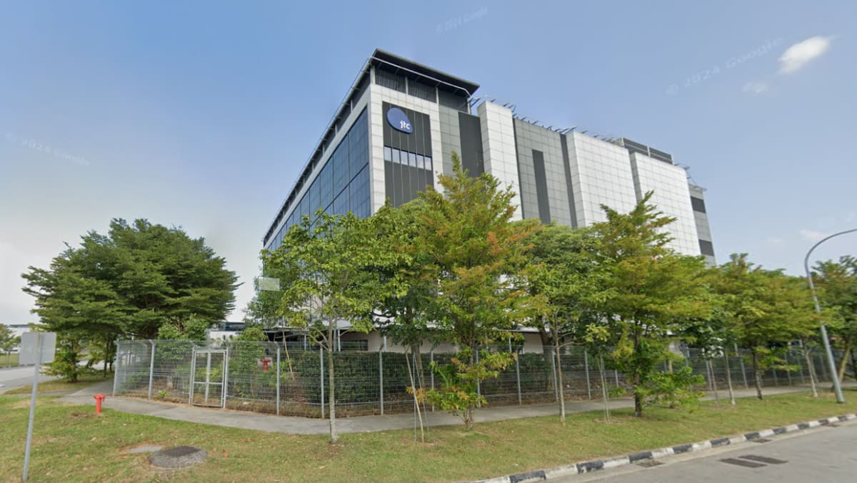
In JTC nanoSpace@ Tampines, a new$ 500 million ( US$ 374 million ) semiconductor fabrication research and development facility will start operating in 2027.
Singapore must invest in research and development to spur innovation in the sector, according to deputy prime minister and trade and industry minister Gan Kim Yong on Thursday ( Mar 6 ).
The national facility will be built to support advanced semiconductor research and innovation, according to the Agency for Science Technology and Research ( A*STAR ). It is a component of the National Semiconductor Translation and Innovation Centre ( NSTIC ) program’s subsequent phase, which was first announced last year.
Mr. Gan outlined the Ministry of Trade and Industry’s ( MTI ) spending plans for the year by stating that semiconductor manufacturing facilities typically require significant upfront investments.
” Businesses, especially the smaller ones, may have trouble gaining access to silicon experience and facilities during their R&, D and captain manufacturing,” he said.  ,
A*STAR may expand NSTIC to include more semiconductor technology and expand its scope.
The R&, D construction facility, which was first announced at Budget 2025,  , did first concentrate on superior packaging technologies, which combine various semiconductor components into a single unit to produce chips more quickly, more potent, and more effectively.
It will serve as a shared resource and will contain 12-inch ( 300mm ) industry-grade tools that can speed up production and reduce costs.
Both the government and the private sector may have access to cutting-edge tools, fabrication facilities, and tools. To reduce pollution by airborne particles, cleaner rooms are remarkably controlled environments used in transistor advancement.  ,
This will be especially advantageous for SMEs and start-ups because it will give them access to crucial silicon facilities, which would otherwise necessitate significant honest investments, A*STAR said.
Mr. Gan further stated that the hospital might encourage new partnerships.
The organization cited the R&, D Fab as a means of bridging the “lab-to-fab” difference between semiconductors and smaller-scale manufacturing facilities.
Companies can collaborate with another ecosystem players or collaborate with higher education institutions to develop experienced professionals.
Through this R&, D Fab, there may also be opportunities for Singapore startups and small and medium-sized enterprises ( SMEs ) to be integrated into the supply chain for advanced semiconductor technologies, according to A*STAR.