TOKYO – In the latest move against China, the US government has imposed export controls on a next-generation semiconductor material that was initially developed in Japan.
On August 12, the Bureau of Industry and Security (BIS) of the US Department of Commerce – as part of a wholesale move toward additional tech sanctions – issued a ruling that identified gallium oxide semiconductor substrates as an “emerging and foundational” technology “essential to the national security of the United States.”
Gallium oxide is a promising material for the fabrication of more efficient power devices used in electric vehicles and other – including military – applications. Tellingly, one major investor in the leading US company in the field is the US Department of Defense.
As explained by Taiyo Nippon Sanso, a Japanese company participating in its commercialization, “Its theoretical performance as a power device is far higher than that of silicon, and also exceeds that of silicon carbide and gallium nitride, making this an excellent material.”
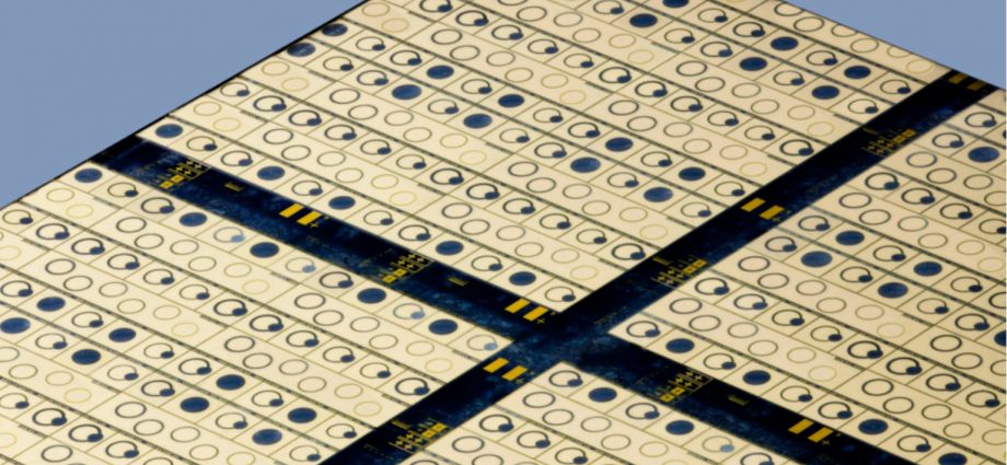
Power semiconductors supply and control electricity used to run motors and charge batteries by converting electric power from AC to DC and adjusting voltages to appropriate levels. Most of those in use today are made from silicon, silicon carbide and gallium nitride. Gallium oxide is only now moving from R&D to initial commercial application.
The development of gallium oxide wafers and devices is underway in the US, Japan, Europe, South Korea, Taiwan and China. While the US government is ringing alarms about gallium oxide’s national security implications, the Japanese are leading way to its commercialization.
Three companies stand out as developers and manufacturers of gallium oxide substrates, wafers and devices, namely Kyma Technologies of the US and FLOSFIA and Novel Crystal Technology of Japan. Let’s examine each of these early leaders in the material.
Kyma Technologies
Founded in 1998 as a spin-off from North Carolina State University, Kyma Technologies is situated in the Research Triangle area of North Carolina with its headquarters in Raleigh. Its business is focused on wide bandgap semiconductors for specialty lighting, laser diodes and power electronics.
The company manufactures gallium nitride, aluminum nitride, gallium oxide and other types of semiconductor substrates, epitaxial wafers and devices, vapor deposition and other crystal growth systems while provideing design, fabrication and other engineering services. It added gallium oxide to its product line in 2016.


Kyma Technologies’ website features a one-inch gallium oxide substrate, five gallium nitride and aluminum nitride wafer products and gallium nitride switches. It lists email addresses for sales in America, China, Europe, Japan, Korea, Taiwan and elsewhere.
Its shareholders include venture capital funds as well as the US Department of Defense.
FLOSFIA
Founded in 2011 as a spin-off from Kyoto University, FLOSFIA specializes in gallium oxide semiconductor devices fabricated using its own mist chemical vapor deposition (CVD) technology. It claims to have achieved the world’s first mass production of a gallium oxide power device and to have produced the world’s most efficient (lowest power loss) gallium oxide diode (semiconductor switch).
Having commercialized its power devices, FLOSFIA now plans to start high-volume shipments to the auto industry with production outsourced to Japanese semiconductor makers.
FLOSFIA’s shareholders include Kyoto University Innovation Capital, University of Tokyo Edge Capital and other investment funds along with private Japanese corporations including Brother Industries (electronic equipment), Yaskawa Electric (motors and industrial robots), Mitsubishi Heavy Industries (electrical and industrial machinery), DENSO (auto and industrial parts and equipment, and semiconductors; DENSO’S affiliated with Toyota) and Fujimi (abrasives and other materials and equipment used in the production of semiconductors and other electronic devices).
FLOSFIA and DENSO are now collaborating in the development of a “next-generation power semiconductor device expected to reduce the energy loss, cost, size and weight of inverters used in electrified vehicles (EVs)” to “improve the efficiency of EV power control units.” The other industrial shareholders are likely to find their own uses for the product.
Novel Crystal Technology
Novel Crystal Technology is a carve-out from Tamura Corporation, a Japanese maker of electronic components, chemicals and equipment. Tamura claims to have produced the world’s first gallium oxide transistor in 2013, “opening the way to practical application of innovative next-generation semiconductor power devices.”
But the first such transistor was developed the previous year by researcher Masataka Higashiwaki of Japan’s National Institute of Information and Communications Technology (NICT). In 2015, Novel Crystal Technology was established in cooperation with NICT.
Novel Crystal Technology also works with Taiyo Nippon Sanso, Tokyo University of Agriculture and Technology and Japan’s New Energy and Industrial Technology Organization (NEDO).
NICT is a “bridging research institute” in the “promotion project for small and medium-sized enterprises,” a “subsidized project” implemented by NEDO.
In December 2021, after four years of work, NEDO and Novel Crystal Technology announced the development of gallium oxide diodes that “will lead to lower priced and higher performance power electronics” and enable “more efficient and miniaturized power electronics devices such as power converters for photovoltaic power generation, general-purpose inverters for industrial use, and power supplies.”
It plans to outsource manufacturing and commence sales in the second half of 2023.
Novel Crystal Technology shows 2-inch gallium oxide wafers for R&D purposes on its website and 4-inch wafers were broached in a telephone interview. These are sold to customers in Japan, the US, Europe, South Korea and China, with about 30% sold in the domestic market and the remaining 70% shipped overseas.


Novel Crystal Technology’s shareholders include Japanese corporations AGC (glass), Hazama Ando (construction), JX Nippon Mining & Metals, ROHM (semiconductors, including power devices), Shindengen (power semiconductors and related equipment), Torex Semiconductor, Yaskawa Electric, Iwatani Venture Capital and Tamura.
JX Nippon Mining & Metals Corporation is investing in Novel Crystal Technology as part of its long-term plan to expand its business in new materials that contribute to decarbonization. The two companies work together on the development of raw materials for gallium oxide power devices.
Taiyo Nippon Sanso is a Japanese producer of industrial gases and related plants and equipment. Its new strategic businesses include metal organic chemical vapor deposition (MOCVD) systems used in compound semiconductor manufacturing, carbon nanotubes and biotechnology. It works with NEDO and Novel Crystal to develop mass production systems for gallium oxide epitaxial wafers.
Atecom Technology, a Taiwanese manufacturer and seller of silicon ingots and wafers, also deals in gallium oxide. On the Chinese mainland, Xiamen Powerway Advanced Materials (PAM-XIAMEN) is in the early stages of developing the technology. For the time being, neither appears to be a competitive threat to the Japanese or Americans.
Typically, the Japanese have brought overwhelming public and private resources to bear in the development of gallium oxide and are likely to make maximum use of its industrial potential. They are highly unlikely to provide their technical secrets to China, even in the absence of formal US export controls.
The scale of the Japanese effort appears to put Kyma Technologies at a disadvantage, but its technology is comparable and it should benefit from the goverment-backed revival of America’s tech industry. If any player should be worried about being left behind, it is the Chinese – which, of course, is the point of the Commerce Department’s export controls.
We will no doubt be hearing from Kyma Technologies again, even if their work with the US military remains under wraps; what the Japanese military may be doing with gallium oxide is another question. But looking at the FAQs page on Kyma Technologies’s website, we can see:
Q: “Why is gallium oxide getting so much attention?”
A: “Gallium oxide, especially in its beta-form [β-Ga2O3], is an exciting ultra-wide bandgap semiconductor (UWBGS) material due to its tantalizing mix of physical properties that together translate to very high figures of merit [a numerical expression representing performance or efficiency] for a number of high speed electronics and power electronics applications.”
Gallium oxide has a bandgap of 4.5 eV in its beta form (β-Ga2O3), with which Kyma, FLOSFIA and Novel Crystal are primarily working. In comparison, the bandgap of silicon (Si) is 1.1eV and the “wide” bandgaps of silicon carbide (SiC) and gallium nitride (GaN) are 3.3eV and 3.4eV, respectively.
The higher the bandgap, the more efficient the power device. As explained in Electronic Design’s Power Management Series:
“Wide bandgap (WBG) semiconductor materials allow smaller, faster, more reliable power electronic components and with higher efficiency than their silicon-based counterparts. These capabilities make it possible to reduce weight, volume, and life-cycle costs in a wide range of power applications. Harnessing these capabilities can lead to dramatic energy savings in industrial processing and consumer appliances, accelerate widespread use of electric vehicles and fuel cells, and help integrate renewable energy onto the electric grid.”
SiC and GaN are the wide bandgap semiconductors in widespread use today. Ultra-wide bandgap semiconductors have bandgaps greater than GaN. In addition to gallium oxide, they include aluminum nitride and diamond.
While not superior in all respects, gallium oxide has the virtue of being relatively easy and potentially cheaper to manufacture. It should make inroads into the power device market over the next several years and could eventually make a major contribution to electric vehicles once economies of scale are achieved.
Follow this writer on Twitter: @ScottFo83517667